- 您现在的位置:买卖IC网 > Sheet目录1995 > FT7521L6X (Fairchild Semiconductor)IC RESET TIMER 7.5SEC 6MICROPAK
2009 Fairchild Semiconductor Corporation
www.fairchildsemi.com
FT7521
Rev. 1.0.8
2
FT7521
—
Re
set
Ti
mer
with
Fi
x
ed
De
lay
and
Rese
t
Pulse
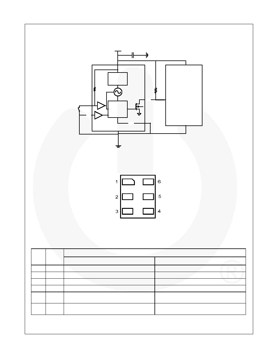
Recommended Application Diagram
Open-Drain Output
Digital Logic &
Counter
Voltage
Reference
/SR0
DSR
/RST1
50k
RPU
VCC
TEST
10k
Baseband or PMIC
100nF
Oscillator
Figure 2.
Recommended Application Diagram
Pin Configuration
Figure 3.
Pad Assignments (Top-Through View)
Pin Definitions
Pin #
Name
Description
Normal Operation
Zero-Second Factory-Test Mode
1
/RST1
Open-drain output, active LOW
2
GND
3
/SR0
Reset Input with Integrated pull-up, active LOW
Reset input with integrated pull-up, active LOW
4
VCC
Power supply
5
DSR
Delay selection input; tie to GND during normal
operation.
Delay selection input. Pull HIGH to enable zero-
second delay for factory test.
6
TEST
Used for device testing; tie to GND during
normal operation.
Used for device testing; tie to GND during
normal operation.
Note:
1.
This pin must always be tied to either GND or VCC. It must not float.
发布紧急采购,3分钟左右您将得到回复。
相关PDF资料
FT7522L6X
IC RESET TIMER 6-MICROPAK
FT8010UMX
IC RESET TIMER CONF DELAY 10UMLP
FTS125-COO-010.0M
IC GPS BASED TIMING MOD (OCXO)
FTS125-CTV-010.0M
IC GPS BASED TIMING MOD (TCXO)
FTS250-010.0M
IC GPS BASED TIMING MOD (TCXO)
FTS375-010.0M
IC GPS BASED TIMING MOD (OCXO)
HD3-6408-9Z
IC ASMA ADT CMOS 1.25MHZ 24DIP
HI1-565AJD-5
CONV D/A 12BIT 6.7MHZ 24-DIP
相关代理商/技术参数
FT7522
制造商:FAIRCHILD 制造商全称:Fairchild Semiconductor 功能描述:Reset Timer with Fixed Delay and Reset Pulse
FT7522L6X
功能描述:计时器和支持产品 ResetTimer w/ Delay
RoHS:否 制造商:Micrel 类型:Standard 封装 / 箱体:SOT-23 内部定时器数量:1 电源电压-最大:18 V 电源电压-最小:2.7 V 最大功率耗散: 最大工作温度:+ 85 C 最小工作温度:- 40 C 封装:Reel
FT-7600
制造商:GC Electronics 功能描述: 制造商:Winchester Electronics 功能描述:
FT762-03004-043
制造商:Japan Aviation Electronics (JAE) 功能描述:
FT762-03004-055
制造商:Japan Aviation Electronics (JAE) 功能描述:
FT762-03118-044
制造商:Japan Aviation Electronics (JAE) 功能描述:
FT765-03004-054
制造商:Japan Aviation Electronics (JAE) 功能描述:
FT-8
制造商:ITT Interconnect Solutions 功能描述:FT-8 / 995-2000-073 / Tools